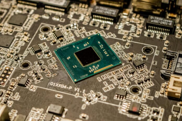
Semiconductors are fundamental components in modern electronics, enabling the functionality of devices ranging from smartphones to spacecraft. The fabrication process of semiconductors involves intricate steps that integrate physics, chemistry, and engineering principles. Here’s an in-depth look at the steps involved in semiconductor fabrication.
1. Crystal Growth:
- Starting Material: High-purity silicon (Si) is the primary material used due to its semiconductor properties.
- Czochralski Process: A silicon seed crystal is dipped into molten silicon and slowly pulled out, forming a cylindrical ingot. This process ensures high crystalline quality.
- Slicing: The ingot is sliced into thin, circular wafers using diamond saws, with each wafer serving as a substrate for semiconductor devices.
2. Wafer Preparation:
- Cleaning: Wafers undergo rigorous cleaning processes using chemicals and ultrapure water to remove contaminants and particles.
- Polishing: Mechanical and chemical polishing techniques are employed to achieve a smooth surface, essential for subsequent processing steps.
3. Deposition:
- Thin Film Deposition: Layers of various materials (e.g., silicon dioxide, silicon nitride) are deposited onto the wafer’s surface using techniques such as chemical vapor deposition (CVD) or physical vapor deposition (PVD).
- Uniformity Control: Precise control of deposition parameters ensures uniform thickness and composition of deposited layers across the wafer.
4. Photolithography:
- Photoresist Application: A photoresist material is applied uniformly over the wafer’s surface.
- Mask Alignment: A photomask, containing the pattern of the semiconductor device, is aligned and placed over the wafer.
- Exposure: The wafer is exposed to ultraviolet (UV) light through the photomask, transferring the pattern onto the photoresist layer.
5. Etching:
- Pattern Transfer: Areas of the photoresist layer exposed to UV light are chemically etched away, exposing underlying materials on the wafer.
- Selective Etching: Different etching techniques, such as wet etching or plasma etching, selectively remove materials according to the pattern defined by the photoresist.
6. Doping:
- Ion Implantation: Dopant atoms (e.g., boron, phosphorus) are precisely implanted into specific regions of the semiconductor wafer to modify its electrical properties.
- Activation Annealing: The wafer undergoes a heat treatment process (annealing) to activate dopant atoms and repair any damage caused during ion implantation.
7. Metallization:
- Metal Deposition: Thin metal layers (e.g., aluminum, copper) are deposited onto the wafer’s surface to create electrical contacts and interconnects between different semiconductor components.
- Patterning: Photolithography and etching processes are used again to define the metal interconnects and contacts.
8. Insulation and Passivation:
- Dielectric Deposition: Insulating layers (e.g., silicon dioxide, silicon nitride) are deposited to isolate and protect semiconductor components from electrical interference.
- Surface Passivation: Techniques like plasma-enhanced chemical vapor deposition (PECVD) are used to passivate the semiconductor surface, improving device reliability and performance.
9. Testing and Quality Control:
- Electrical Testing: Each wafer and individual semiconductor device undergoes rigorous testing to ensure functionality, performance, and reliability.
- Defect Inspection: Advanced inspection techniques, such as scanning electron microscopy (SEM) and optical inspection systems, detect and characterize defects that could impact device operation.
10. Packaging and Assembly:
- Die Separation: Wafers are diced into individual semiconductor devices (chips).
- Packaging: Each chip is mounted onto a package and wire bonded or flip-chip bonded to connect it to external leads or pins.
- Encapsulation: Chips are encapsulated in protective materials (e.g., epoxy resin) to safeguard against environmental factors and mechanical stress.
11. Final Testing and Yield Optimization:
- Functional Testing: Packaged semiconductor devices undergo final electrical testing to verify functionality under operating conditions.
- Yield Enhancement: Statistical process control (SPC) and yield optimization techniques are employed to maximize the number of defect-free devices per wafer.
12. Distribution and Integration:
- Integration into Electronic Systems: Finished semiconductor devices are integrated into electronic systems during device manufacturing, such as in computers, smartphones, automotive electronics, and industrial equipment.
- Lifecycle Management: Continuous monitoring and improvement processes ensure ongoing quality and performance of semiconductor devices throughout their lifecycle.
Advanced Technologies and Future Directions:
- Nanotechnology: Advances in nanoscale fabrication techniques enable the production of smaller, more efficient semiconductor devices.
- Materials Innovation: Exploration of new semiconductor materials (e.g., gallium nitride, silicon carbide) with superior electrical properties for specific applications like power electronics and high-frequency devices.
In conclusion, semiconductor fabrication is a highly sophisticated and precise process that combines scientific knowledge with engineering expertise. Each step in the fabrication process plays a critical role in producing semiconductor devices that power the technological innovations of today and tomorrow.

